Agnitron Technology introduces the Blue & UV Fiberoptic Reflectometer for In-situ Monitoring.
Agnitron Technology of Chanhassen, MN has begun providing its customers with an advanced Blue & UV reflectometer to provide growth rate (or etch rate) of Ga2O3 & GaN including its different alloys. Moreover it measures the thickness (or etch depth) of the epitaxial films. It spans a host of oxide materials, important in the research community more recently.
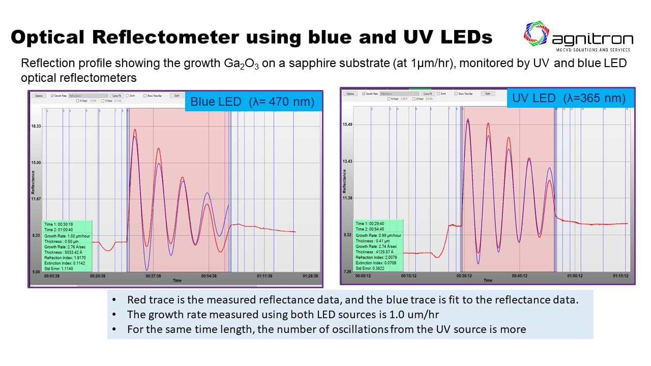
To drive maximum flexibility, the unit can be configured with several different wavelength LEDs. For Ga2O3 & GaN alloys either 405nm or 365nm is most common. Customers can select the wavelength of choice and switch between them at desired. In the next months, a 280nm LED will be tested to support customers growing other ultra-wide bandgap materials. In addition, the reflectometer is equipped with a powerful analytical software package based on the Imperium™ platform. It is synced with Imperium™ to provide a comprehensive display of the time cycles for correlation of the dynamic layers and the reflectometer outputs. The recipes, the growth, the reflectance output, and the analysis are all linked for the Agnitron customer. It is displayed in real-time, or the customer may analyze the data post-run. A simulation model to determine the growth rate and the film thickness is shown below within Imperium™.
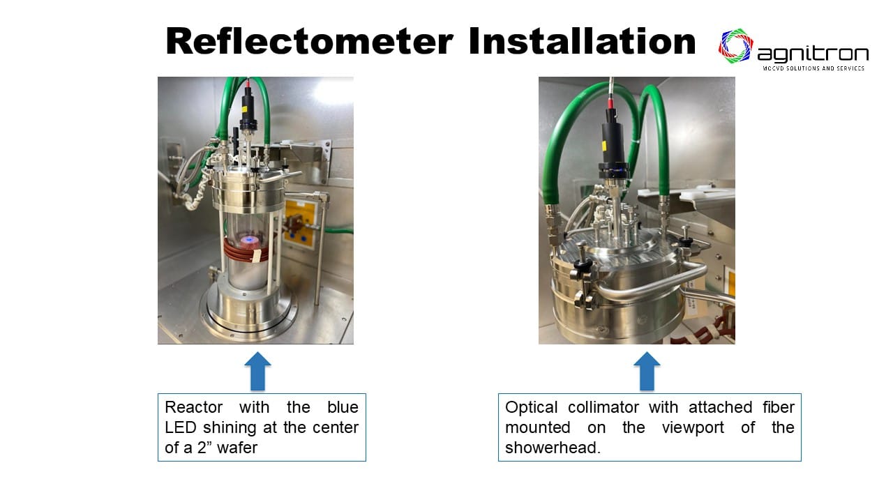
Pictured below is the new reflectometer on Agnitron’s popular Agilis 100 MOCVD tool using the BLUE version seen at the center of the wafer positioned on susceptor. A corresponding display of the growth is also shown. The apparatus is easy to install, configure, change wavelengths, and calibrate. A signature feature of Agnitron’s products.
The device can be configured for a variety of OEM tools as well. Contact Agnitron Technology at sales@agnitron.com with any questions or further information requests.
Agnitron Technology, Inc. is a compound semiconductor technology company and supports MOCVD equipment related needs of R&D and production users. We strive to deliver products and services to enable development of advanced semiconductor material, device technologies, and products which improve quality of life and the environment.

