
Researchers design HEMTs with increased breakdown voltage at high temps
6 March 2013
Air-bridge to improve field-plate performance for nitride HEMTs
Researchers in China and Canada have developed air-bridge field plates for nitride semiconductor high-electron-mobility transistors (HEMTs) that increase the breakdown voltage and offer more stable performance at raised temperatures [Xie Gang et al, Chin. Phys. B Vol. 22, p026103, 2013]. The work was carried out between Zhejiang University, University of Toronto, and University of Electronic Science and Technology of China.
Field plates are used to manipulate electric field distributions in HEMTs. With suitable designs, the peak value of the electric field can be reduced, allowing greater voltages to be sustained. However, such structures can add parasitic side-effects such as increased capacitance between the terminals. The air-bridge field plates were proposed as an attempt to reduce some of these effects.
The researchers produced HEMTs with conventional field plates (CFP, Figure 1a) and air-bridge field plates (AFP, Figure 1b). Both FPs were connected to the source terminal. The aluminium gallium nitride (AlGaN) barrier in the epitaxial structure had 28% Al mole fraction. The sheet carrier density and mobility from Hall measurements were 1.1×10¹³/cm2 and 1800cm2/V-s, respectively.
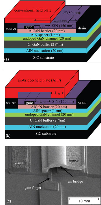
Figure 1: Cross-sectional view of proposed HEMT structure: (a) with a CFP, where LFP is FP length. (b) AlGaN/GaN HEMT with novel AFP, where LGF, LM and LGD are the gate-to-air-bridge field-plate distance, air-bridge footprint width, and gate-drain distance (drift region), respectively. (c) SEM view of fabricated novel AFP HEMT.
The ohmic source-drain contacts of the devices consisted of titanium/aluminium/nickel/gold annealed at 850°C for 30 seconds in nitrogen. The Schottky gate electrode was platinum. Silicon nitride passivation was applied using plasma-enhanced chemical vapor deposition (PECVD). The field-plate structures were made from 1000nm-thick gold.
“The fabrication process for the AFP HEMT is fully compatible with the commercial RF GaN technology without the need for any additional photolithography or processing steps,” the researchers report.
Using an air-bridge greatly reduced the gate-source capacitance compared with conventional field plates due to air having the lowest dielectric constant of essentially 1.
Measurements and simulations with varied field-plate parameters suggested optimum values of 2μm for the AFP footprint (LM) and gate-FP distance of 0.5μm (LGF). For the CFP devices, the optimum FP length (LFP) was 1.2μm. The effects of the varying these parameters in simulations were to alter the heights of field peaks near the gate and FP edges. It is these field peaks that are responsible for device breakdown.
The other device parameters were a source-gate distance of 1.1μm, gate length of 0.8μm, gate width of 80μm, and gate-drain distance of 6μm.
The off-state breakdown (-5V gate potential) was 37V for a HEMT without FP, 125V with optimum CFP, and 375V with optimum AFP. The drain leakage for the HEMT without FP was 10-2A/mm before breakdown. A similar current level was seen with the CFP. However, for the AFP device, the drain leakage was one order of magnitude lower.
The researchers also carried out measurements at raised temperatures (Figure 2). The breakdown performance with AFP is almost constant up to 400K. The researchers believe that this is because the AFP suppresses the drain side gate-edge electric-field-induced gate-to-channel hot carrier injection. Increasing the temperature to 450K reduced the breakdown to 320V. The lower breakdown was attributed to increased gate leakage at higher temperatures.
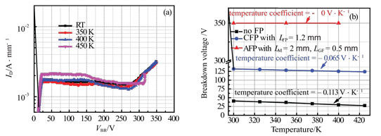
Figure 2: Measured breakdown voltage with different temperatures for (a) HEMT with AFP, (b) temperature coefficient of breakdown voltage for conventional HEMT (no FP), HEMT with CFP, HEMT with AFP, respectively.
By contrast, HEMTs without FP and with CFP showed degraded breakdown with raising the temperature at rates of -0.113V/K and -0.065V/K, respectively.
http://iopscience.iop.org/1674-1056/22/2/026103
Source: http://www.semiconductor-today.com