
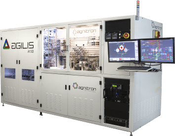
Five Agilis β-Ga2O3 MOCVD Systems In Production by Agnitron To Fulfill New Orders
Agnitron’s Agilis MOCVD β-Ga2O3 configuration is now available for general market customers and extends the same system configurations as have been used by the Agnitron team to produce reported works in recent articles and presentations*. The configuration has been extended to customers in response to interest stimulated by Agnitron’s ground breaking β-Ga2O3 MOCVD growth work and is capable of delivering state-of-the-art growth performance. This special Agilis β-Ga2O3 configuration is available with single or multi-wafer loading capacity. Of the 5 systems currently in production at Agnitron, three of these systems offer single wafer loading and the other two multi-wafer loading. Provided the flexibility of the Agilis platform, the single wafer systems are designed to be field upgraded to a multi-wafer reactor with minimal efforts.
This Agilis β-Ga2O3 configuration is ideal for customers interested in achieving advanced growth capabilities to support device related R&D efforts in the rapidly growing field. This new reactor set and equipment configuration is based on years of development by Agnitron and was supported by advanced multi-physics process modeling in addition to experimental activities. The team’s efforts resulted in material growth performance not previously known to be possible by MOCVD and represent exciting developments for β-Ga2O3 technologies. Agnitron’s system will support high growth rates which is significant as MOCVD is an industrial compatible process proven capable of large area growth with sharp layer interfaces and smooth surface morphologies – all important considerations for future technology commercialization efforts. Furthermore, Agnitron’s configuration is capable of supporting a broad range of process conditions for studying wider and narrower bandgap alloys, heterostructures, sharp delta-doped profiles and regrowth processes which are all critical for device development programs. Now with a strong industrially scalable material growth foundation the stage is set for improving our understanding of possibilities for β-Ga2O3 power and extreme environment electronics device applications.
A number of recent publications on the topic of MOCVD growth of β-Ga2O3 by Agnitron detail expertise and capabilities held by the team and serve as an outline of foundational growth capabilities possible with Agnitron’s Agilis β-Ga2O3 MOCVD Systems. More information is available in the articles listed at the end of this posting.
Agnitron Technology, Inc. is a compound semiconductor technology company and supports MOCVD equipment-related needs of R&D and production users. Agnitron’s Agilis Series MOCVD equipment offers a menu of options for reactor (single or dual) designs, source configurations, metrology and many other performance items for advanced and flexible R&D capabilities. Agilis offers configurations which support material growth capabilities for III-N, As/P, oxide, 2-D/TMD and many other related materials. The Agilis β-Ga2O3 configuration with single or multi-wafer loading capacity reactor options is now available for purchase. Agnitron also performs contract III-N and oxide R&D services at their MOCVD growth laboratory in Eden Prairie, MN. Contact sales@agnitron.com for more information about our products or services.
*Supporting References for Agilis β-Ga2O3 MOCVD System Performance:
- Upcoming: “MOCVD growth of high-quality epitaxial b-Ga2O3 and related alloy structures” F. Alema, R. Miller, A. Osinsky, A. Mauze, J. Speck, M. Bogdanov, A. Lobanova, R. Talalaev, and A. Galyukov, ICMOVPE-XIX June 2-8, 2018 Nara, Japan.
- Upcoming: “Advances toward industrial compatible epitaxial growth of b-Ga2O3 and alloys for power electronics” Miller, F. Alema and A. Osinsky, CS MANTECH May 7-10, 2018 Austin, TX.
- “β-Ga2O3 and b-(Alx,Ga1-x)2O3 by MOCVD”, A. Osinsky, Session 9: Epitaxy and Deposition, WOCSEMMAD 2018, San Diego, CA, Feb 21, 2018.
- “Growth of Ga2O3 and AlGaO epitaxial structures by MOCVD”, A. Osinsky, Invited Talk, Gallium Oxide II: Thin Films and Epitaxy, Oxide-based Materials and Devices IX, SPIE Photonics West, San Francisco, CA, Jan 28, 2018.
- “Fast growth rate of epitaxial β–Ga2O3 by close coupled shower head MOCVD Growth” F. Alema, B. Hertog, A. Osinsky,P. Mukhopadhyay, M. Toporkov, W. V. Schoenfeld, J. Cryst. Growth 475 (2017) 77.
- “Bandgap Engineering and MOCVD Growth of High-Quality β-(Al,Ga)2O3/ Ga2O3 Heterostructures for Power Switches” A.Osinsky, F. Alema, B. Hertog, E. Ahmadi, F. Wu, J. Speck, B. H Nieters, T. Vogt, MRS Fall 2017, Boston, MA.
- “High-Quality Epitaxial β-Ga2O3Growth by Close Coupled Showerhead MOCVD” F. Alema, B. Hertog, A. Osinsky, E. Ahmadi, F. Wu, J. Speck, M. Bogdanov, A. Lobanova, R. Talalaev, A. Galyukov, MRS Fall 2017, Boston, MA.
- “Experimental Study and Modeling of Ga2O3Epitaxial Growth by MOCVD in a CIS Reactor”, M. Bogdanov, A. Lobanova, R. Talalaev, A. Galyukov, F. Alema, B. Hertog, and A. Osinsky, IWGO 2017, Parma, Italy.
- “Vertical solar blind Schottky photodiode based on homoepitaxial Ga2O3 thin film” F.Alema, B. Hertog, A. Osinsky,P. Mukhopadhyay, M. Toporkov, W. V. Schoenfeld, E. Ahmadi, J.Speck, Proc. SPIE 10105, Oxide-based Materials and Devices VIII, 101051M.
- “Epitaxial Growth of Ga2O3By MOCVD Using Oxygen: Experimental Study and Model Verification” M. Bogdanov, A. Lobanova, R. Talalaev, A. Galyukov, F.Alema, B.Hertog, A. Osinsky, ACCGE-21, Santa Fe, NM.
- “Epitaxial β-Ga 2O 3 thin Film by Metal Organic Chemical Vapor Deposition” F.Alema, B. Hertog, O. Ledyaev, G. Thoma, R. Miller, A. Osinsky, P. Mukhopadhyay, W.V. Schoenfeld, MRS Fall 2016, Boston, MA.
- “MgZnO Grown by Molecular Beam Epitaxy on N-Type ß-Ga2O3 for UV Schottky Barrier Solar-Blind Photodetectors” M. Toporkov, P. Mukhopadhyay, H. Ali, V. Beletsky, F. Alema, A. Osinsky, W.V. Schoenfeld, Proc. SPIE 10105, Oxide-based Materials and Devices VIII, 101051N.