
Agnitron Technology and Arizona State University Ga2O3 etching accomplishments highlighted in latest issue of Compound Semiconductor Magazine
Controllable etching of Ga2O3 has been featured in Compound Semiconductor Magazine this month. Ga2O3, an important and increasingly studied ultra- wide bandgap material for next generation power devices is a focus of both Agnitron Technology and ASU.
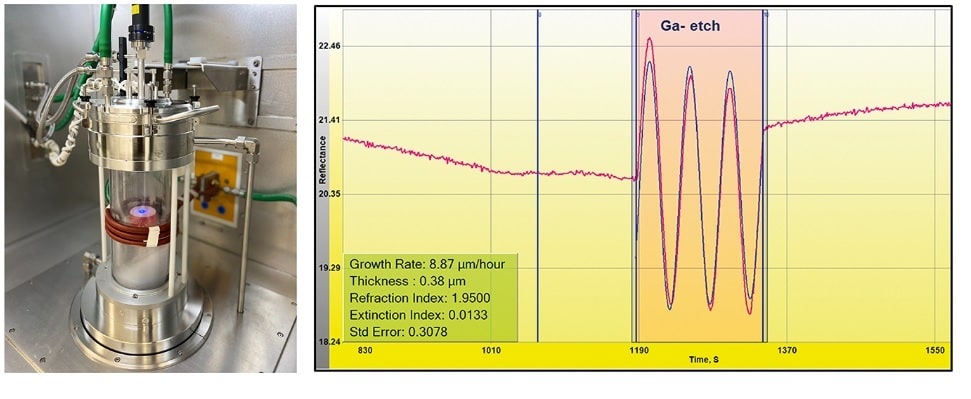
The article details the joint work of Agnitron’s chief scientist, Fikadu Alema and Professor Nidhin Kurian Kalarickal of Arizona State University. It reviews both groups’ effort to study the in-situ etching of Ga2O3 in an Agilis 100 oxide growth system as well as techniques to measure the speed and depth of the etching.
Agnitron produces not only the MOCVD systems to grow and etch ultra-wide bandgap materials but also the metrology tools to measure the growth rate, thickness, and etch-rate while processing the wafers. With Agnitron’s multi-wavelength reflectometry outfitted on the tools, scientists can now do the growth and etching of Ga2O3 controllably to further develop advanced power devices.
Their work is outlined in the article found in Compound Semiconductor Magazine.
https://compoundsemiconductor.net/article/117370/Excelling_in_the_etching_of_gallium_oxide
Agnitron is the world leader in commercially available Ga2O3 MOCVD tools and holds the world-record for mobility and UID MOCVD grown Ga2O3 films.